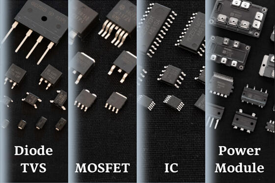
Silicon Limit
There is a limit value known as the “silicon limit” (theoretical limit) which is the limit value at which “RDS(ON) cannot be decreased further” even if all resistance other than the drift layer is decreased infinitely close to 0 due to the remaining resistance in the drift layer.
RDS(ON) of the planar gate MOFET is said to be proportional to VDSS raised to 2.5 as shown by the calculation : VDSS2.5 ∝ RDS(ON).
VDSS 2 times ⇒ RDS(ON) 5.6 times
VDSS 10 times ⇒ RDS(ON) 316 times
There is still some margin left until the theoretical limit is reached for low VDSS MOSFETs, however high VDSS MOSFETs nearly reached the theoretical limit a long time ago, and there is significant demand for a new breakthrough for high VDSS MOSFETs.
⇒Super junction structures are a new technology for exceeding this theoretical limit while continuing to use Si.
RDS(ON) decreasing benefits of super junction structures
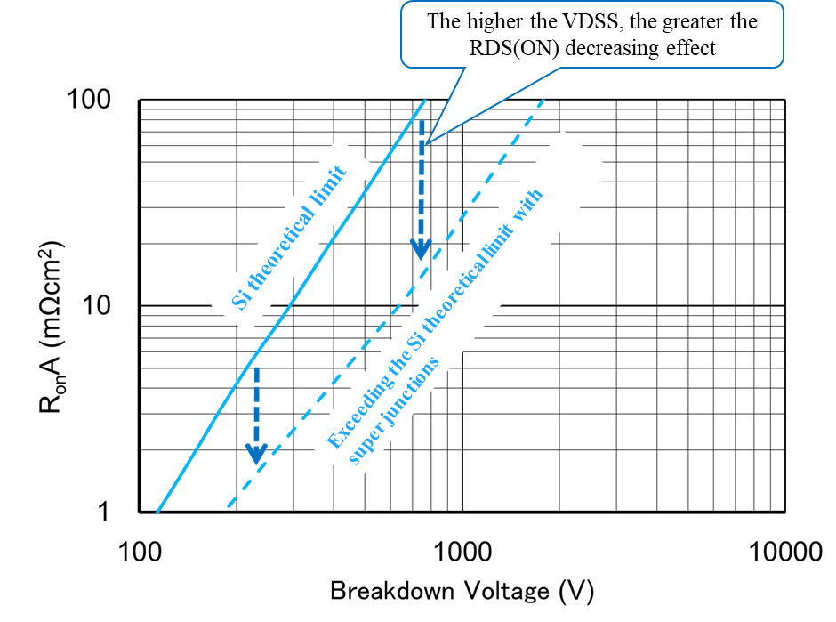
* SJ-MOS have exceeded the silicon limit.
Super junction principles
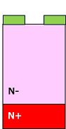
Conventional structure MOSFETs
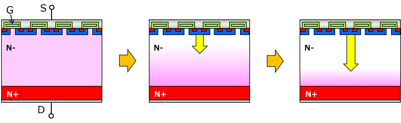
The depletion layer expands based on the applied voltage and this generates the VDSS. Depletion layer expansion = depletion layer thickness, so in high VDSS MOSFETs the impurity concentration in the drift layer cannot be increased. For this reason, the higher the VDSS, the higher the drift layer resistance and therefor the higher the RDS(ON).
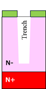
Super junction structure MOSFETs
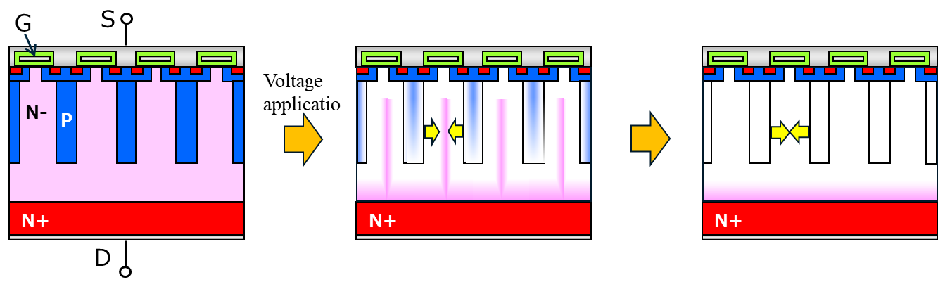
The N layer and P layers are arranged vertical trenches in the drift layer, so that when voltage is applied the depletion layers expand horizontally, and soon merge to form a depletion layer equal to the depth of the trenches.
The depletion layer only expands to half the pitch of the trenches, so a depletion layer is formed with a thickness equal to the depth of the trenches. The expansion of the depletion layer is small and good, allowing for an approximately 5 time increase in the drift layer impurity concentration, which in turn makes it possible to decrease RDS(ON).
From this principle, we can see that making trenches and trench pitch as small and deep as possible is efficacious. This allows for generation of VDSS using a mechanism that differs from conventional MOSFETs, or to put it another way, allows for performance which exceeds the silicon limit.
Differences as viewed from manufacturing methods
Conventional structure MOSFETs
-
-
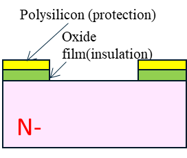
- ① Oxide film is applied to N-wafer.
-
-
-
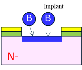
- ② Boron and other impurities are applied to surface.
-
-
-
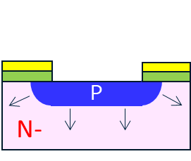
- ③ Impurities are dispersed through heat treatment.They disperse gradually.
-
-
-
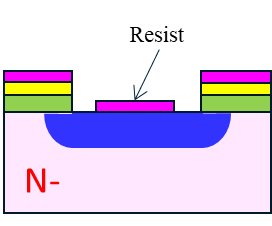
- ④ A resist is applied.
-
-
-
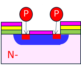
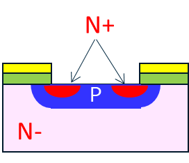
- ⑤ Phosphorous and other impurities are applied to the surface.
-
-
-
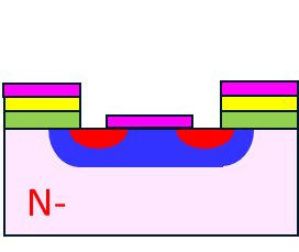
- ⑥ Impurities are dispersed through heat treatment.
-
-
-
- ⑦ Resist is removed.
-
Super junction structure MOSFETs
In recent years, a method has been developed where deep trenches are etched in the N-layer, and P-layer crystals are epitaxially grown in these trenches to form super junction structures.
Trench-filling epitaxial manufacturing method
-
-
- ① Oxide film is applied to the N-substrate.
-
-
-
- ② Deep trenches are etched in the N-layer using dry etching.
-
-
-
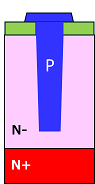
- ③ A P-layer is again epitaxially grown in the etched trenches.
-
-
-
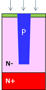
- ④ Any overflow is removed to make the surface level.
-