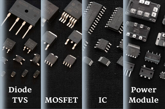
MOSFET characteristic examples (Reference)
(Shindengen Electric Manufacturing Co., Ltd. products)
|
Type No. |
VDSS |
ID |
RDS(ON) |
|---|---|---|---|
|
P60B6SN |
60V |
60A |
5.3mΩ |
|
P4B60HP2 |
600V |
4A |
1.5Ω |
This is a comparison of the RDS(ON) of a low VDSS MOSFET and
high VDSS MOSFET using the same package.
The size of the bare dies is nearly the same, but there is this much of a difference in RDS(ON).
Diode characteristic examples (Reference)
(Shindengen Electric Manufacturing Co., Ltd. products)
|
Type No. |
VRRM |
IF |
VF |
|---|---|---|---|
|
D1FS6A (SBD) |
60V |
2.6A |
0.57V |
|
D1F60A (General Di) |
600V |
1.2A |
0.97V |
Diode VF does not rely on VRRM as much as MOSFET RDS(ON).
What is ON resistance?
ON resistance (RDS (ON)) refers to the resistance from the D terminal to the S terminal which includes the channel resistance as well as other N layer resistance and wire and lead frame resistance, etc.
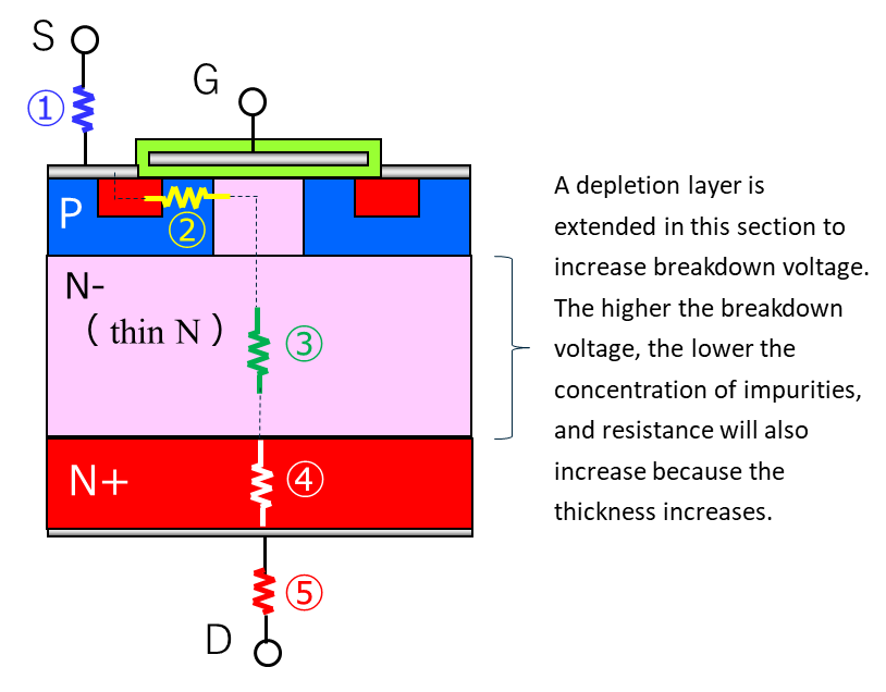
- Wire and lead frame resistance from the S terminal to the S electrode
- Channel resistance
- Drift resistance
- Silicon substrate resistance
- Solder and lead frame resistance from the electrode on the back of the bare die to the D terminal
RDS(ON) details
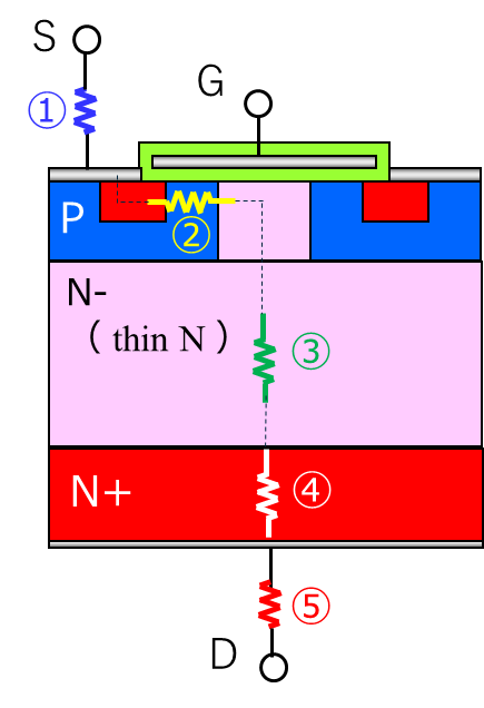
- Wire and lead frame resistance from the S terminal to the S electrode
- Channel resistance
- Drift resistance
⇒This varies greatly between high and low VDSS - Silicon substrate resistance
- Solder and lead frame resistance from the back of the bare die to the D terminal
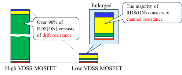
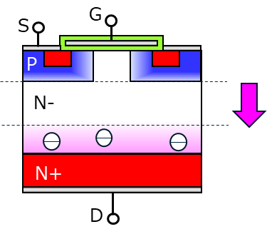
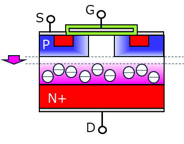
Differences in drift layer between high and low VDSS MOSFETs
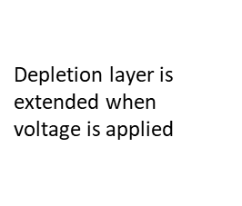
If voltage is applied between D-S, a depletion layer will extend to the N-layer based on the voltage.
The MOSFET VDSS is determined by the size (thickness) of the depletion layer on the N-layer.
High VDSS MOSFET
Low VDSS MOSFET
The MOSFET is designed so that the depletion layer can expand easily, so the N-layer (drift layer) is thick, and the impurity concentration is low.
⇒Resistance value is high when wanting to pass current through
The depletion layer only needs to extend a slight amount, so the N-layer (drift layer) is thin and the impurity concentration is high.
⇒Resistance value is low when wanting to pass current through
From this you can see that there is a “minimum resistance value” based on the required VDSS.
In order to lower RDS(ON)
- Manufacture a single bare die with a large number of clustered cells
⇒This is the basic methodology, however concentrating a large number of clustered cells will increase the bare die size and also increase the cost. - Make each cell as small as possible
⇒If channel length is shortened, the channel resistance per each individual cell will decrease, allowing for a higher concentration of cells on the same bare die area. - Utilize cell layout orientation
⇒This is what the trench technique consists of. Requires specialized processing for etching trenches. - Lower the resistance of components other than the channel
⇒A variety of techniques are utilized to lower resistance including lowering the resistance of the drift layer which increases VDSS, using connectors instead of wires, increasing lead frame and terminal thickness, etc.
Major technologies for lowering RDS(ON)
|
Degree of effectiveness |
Details and aims | ||
|---|---|---|---|
|
Low withstand voltage MOSFETs |
High withstand voltage MOSFETs | ||
|
Process miniaturization |
◎ | 〇 |
The fundamental semiconductor processing technique. Equipment capacity. |
|
Trench gates |
◎ | △ |
Technology where trenches are etches and gates are embedded. |
|
Clips (connectors) |
◎ | △ |
Metallic conductors are used for connections instead of wires. |
|
Super Junction |
✕ | ◎ |
PN stripe structures are created on the drift layer. |
|
Wide Band Gap |
△ | ◎ |
Introduction of new materials such as SiC and GaN. |
Super Junction and Wide Band Gap are technologies for lowering drift layer resistance which are used in high VDSS MOSFETs.
Effects of RDS(ON) and capacitive components on circuit characteristics
Large bare die size
Ron - Low
Capacity - High
Price - High
Small bare die size
Ron - High (4 times)
Capacity - Low (1/4)
Price - Low
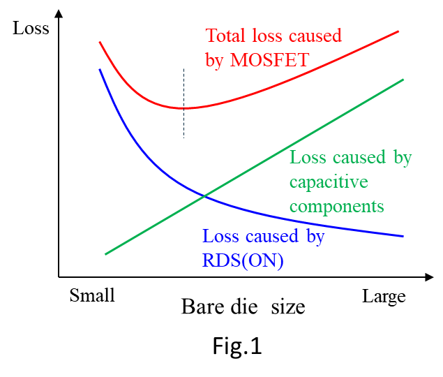
The larger the bare die size, the smaller the RDS(ON) will be, however capacity will also increase by the same amount, so there will be high power loss from switching, drive, etc.
If cost is ignored, the dashed line in the Fig.1 is the optimal performance. Simply having the lowest RDS(ON) is not optimal.