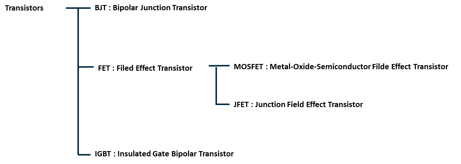
Transistor types
Transistors are a type of component which can amplify signals, turn switches ON and OFF, etc.
They are categorized as follows based on element structure and operation principles.
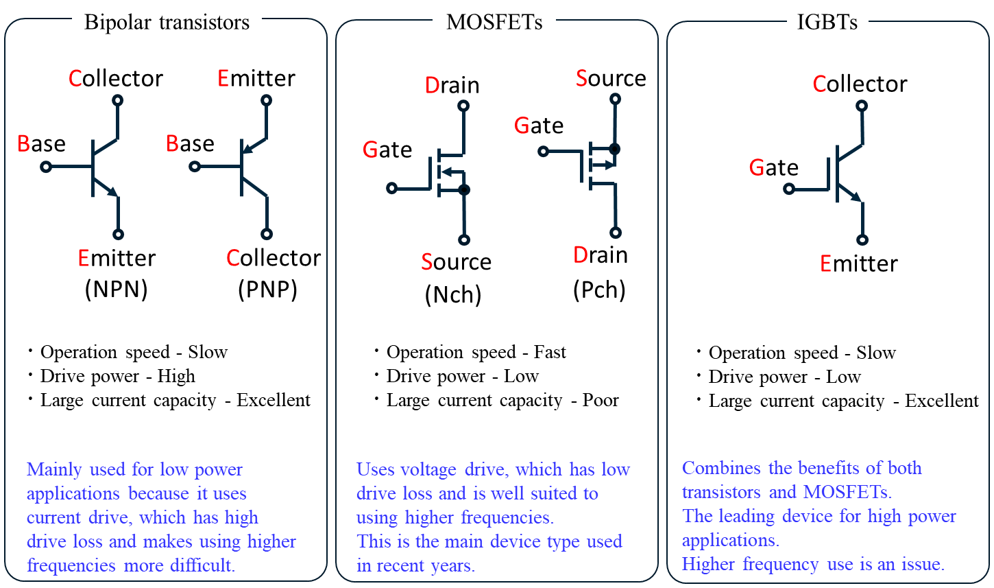
The characteristics of each type of transistor are shown below.
What are MOSFETs
Metal-Oxide-Semiconductor Field Effect Transistor
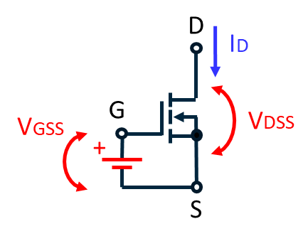
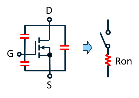
Switch element which switches to a conductive state between D-S if voltage is applied between G-S.
Under optimal conditions Ron=0Ω.
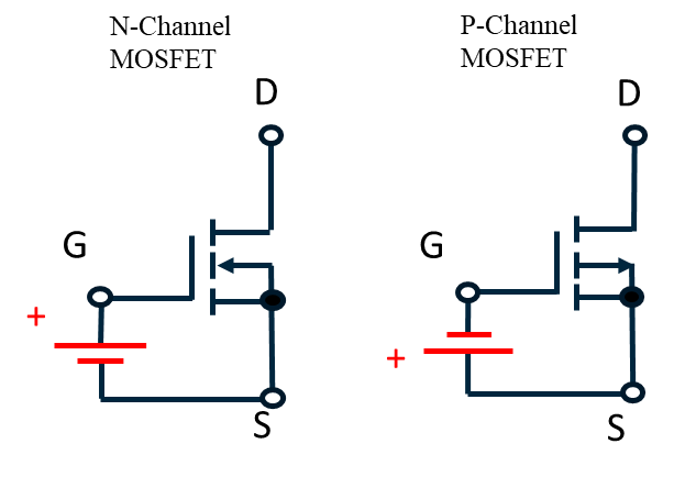
There are N-Channel and P-Channel MOSFET types.
N-Ch turn ON (conductive state) when positive voltage is applied to G (Gate) for S (Source).
P-Ch turn ON (conductive state) when negative voltage is applied to G (Gate) for S (Source).
N-Ch have better performance and are also easier to use in terms of routing, so the majority of the MOSFETs used in the market are N-Ch.
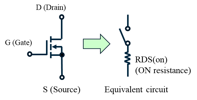
MOSFET operation concept
- Absolute maximum ratings (P8FE10SBK example)
These represent limits which “must not be exceeded under any circumstances” when using the product.
When conditions are not otherwise specified, these are the values at a temperature of 25℃.
|
Item |
Rating |
Unit | Explanation |
|---|---|---|---|
| VDSS | 100 |
V |
Maximum allowable voltage between Drain - Source |
|
ID |
8 | A |
Rated current indicated as direct current. Noted separately for pulse current. |
|
PT |
24 |
W |
Allowable power dissipation. Determined by package heat resistance. |
|
VGSS |
±20 |
V |
Maximum allowable voltage between Gate - Source |
|
Tch |
175 |
℃ |
Maximum allowable channel temperature when MOSFET operates |
-
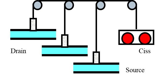
Electrical characteristics (P8FE10SBK example)
These indicate the product’s characteristics specs.
The important items are the RDS(ON) and capacity elements in the following table.
The smaller the value, the better for both items, but this is a tradeoff, so compare Ron × Qg and RDS(ON) × Ciss.
|
Item |
Rating | Unit |
Explanation | ||
|---|---|---|---|---|---|
|
Min. |
Typ. |
Max. | |||
|
RDS (ON) |
- |
79 |
99 | mΩ |
ON resistance |
|
Qg |
- |
16.5 |
- | nC |
Electrical charge required to charge the gate. |
| Ciss | - |
665 |
- | pF |
Combination of the capacity between G-D and the capacity between G-S. |
|
Crss |
- |
26 |
- | pF |
Capacity between G-D. |
|
Coss |
- |
64 |
- | pF |
Capacity between D-S. |
MOSFET operation concept
OFF state
ON state
-
-
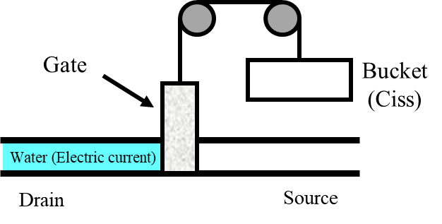
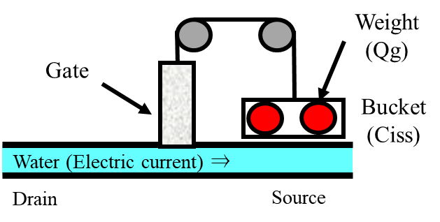
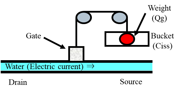
- There is no weight in the bucket, so when the gate is lowered, the water does not flow.
-
-
-
- When weight is added to the bucket, the gate rises and allows the water to flow.
-
If the weight (Qg) is not sufficient, the Gate will only open the part way, so, On resistance (RDS(on) would be high.
-
-
- Water route is narrow (high ON resistance) and gate is light (low Ciss).
-
-
-
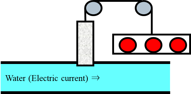
- Water route is wide (low ON resistance) and gate is heavy (high Ciss).
-
If the Ciss is high, a high amount of electrical charge will be needed each time the gate is opened and closed.
This electrical charge will be the “current which charges and discharges the gate”, so it will become power loss (drive loss). In short, the lower the Ciss and Qg, the better.
MOSFET bare die structure concept
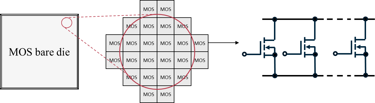
A MOSFET bare die is made up of a large number of clustered MOSFET (cells).
There are a larger number of cells on larger bare die.
⇓
ON resistance is low, and rated current is high.
But this will also make Ciss high.
And the cost will also be high.
So what is a superior MOSFET?
The ON resistance can be lowered by any amount by making a larger MOSFET bare die.
However, this will also result in increasingly higher Ciss and Qg.
-
-
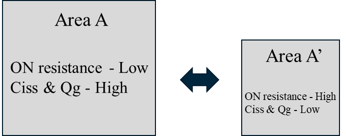
- So, just having “low ON resistance” does not necessarily equal “good performance”.
-
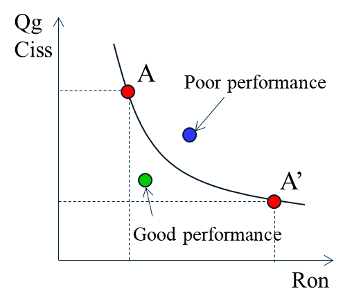
For this reason, a “performance index” called “FOM (Figure of Merit)” when comparing MOSFET performance. FOM types include RDS(ON)×Ciss, RDS(ON)×Qg, RDS(ON)×A, and more.
All of these compare “how low ON resistance is compared to bare die size”.
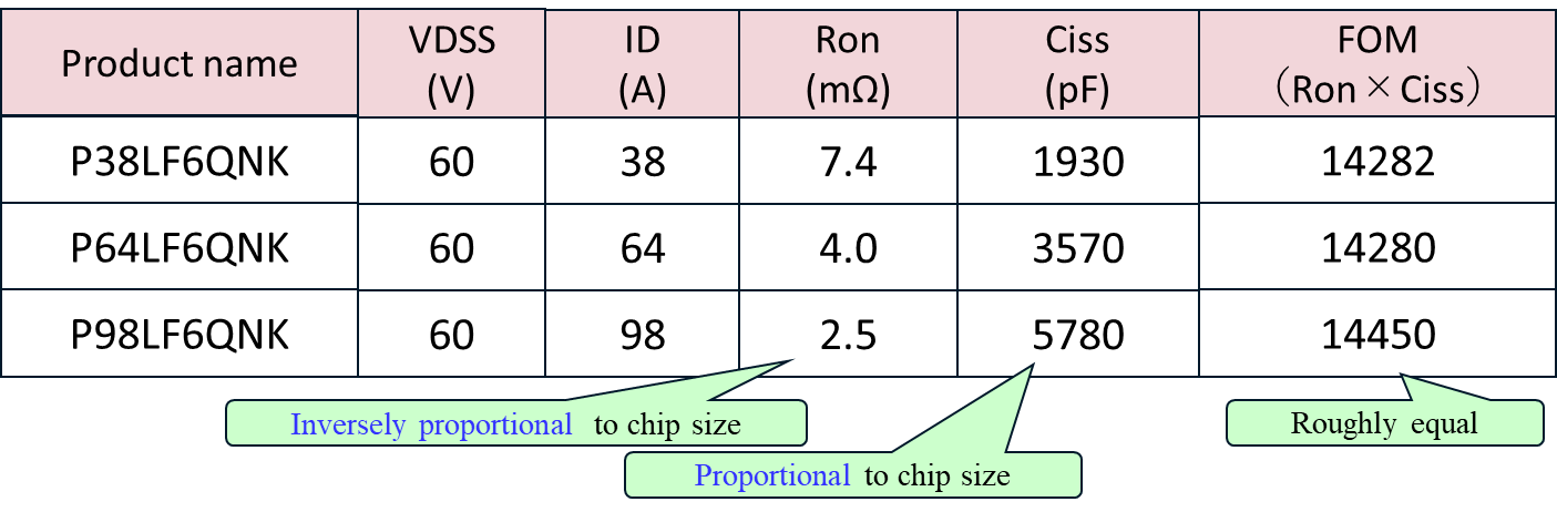
Performance index example
In general, MOSFET from the same manufacturer, same series, and with the same VDSS will have the same design for each unit cell.
The difference in rated current is a result of differences in bare die size, so the larger the bare die, the more cells can be added to lower the ON resistance.