Semiconductor material physical property comparison
| Unit | Si |
4H-SiC |
GaN |
Ga2O3 | Diamond | |
|---|---|---|---|---|---|---|
| Band gap |
eV |
1.12 |
3.26 |
3.39 |
4.8 |
5.47 |
| Electron mobility |
㎠/Vs |
1.12 |
1000 |
900 |
300 |
2200 |
|
Insulation breakdown field intensity |
MV/㎝ |
0.3 |
2.5 |
3.3 |
8 |
10 |
| Thermal conductivity |
W/㎝K |
1.5 |
4.9 |
2 |
4.8 |
20 |
|
BM* |
- |
1 |
340 |
650 |
3400 | 27000 |
| Technology level | - |
Mass |
Partial mass |
Partial mass |
Research stage |
Research stage |
*Baliga's Figure of merit - The larger this value, the higher the potential for lowering the drift layer resistance.
Using a large material for the band gap makes it possible to achieve high insulation breakdown field intensity. Specifically, this means that it is possible to generate a high voltage in a thin depletion layer, so the drift layer can be made thinner and the impurity concentration can be increased, the synergistic benefits of which create the potential to significantly improve the tradeoff between withstand voltage and drift resistance. A figure of merit of 340 SiC, indicates that drift resistance can be reduced to 1/340th using the given material.
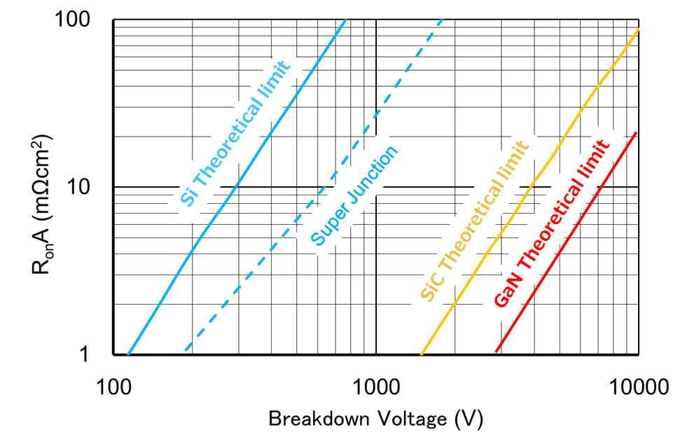
Comparison of theoretical limits by semiconductor materials
Wide band gap semiconductors are semiconductor materials which can greatly reduce ON resistance.
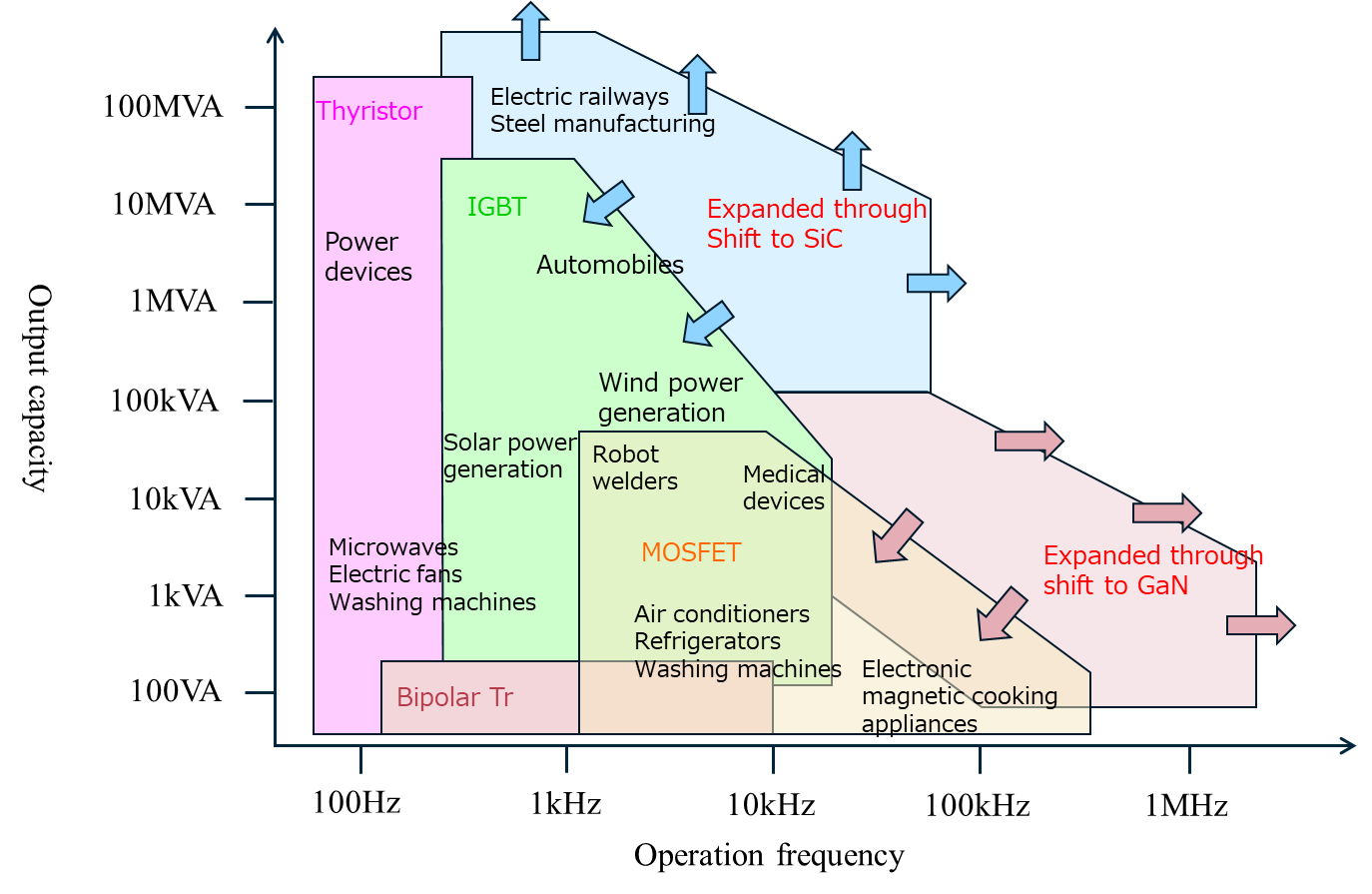
Power device application fields
SiC contributes to higher withstand voltage and higher power, while GaN contributes to higher frequency usage, both of which expand the application fields for power devices.