Movement of electrons and holes in semiconductor
-
-
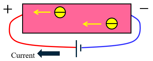
- n-type semiconductor
-
Electrons move toward the plus pole. At this time, current flows in the opposite direction of the electrons’ movement.
-
-
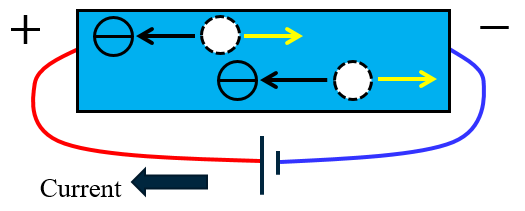
- p-type semiconductor
-
Electrons are what is actually moving, but the holes appear to be moving toward the direction of the minus pole.
As a result, both p-type and n-type semiconductors can have current flow, but they are not as conductive as metal. Therefore, there is no need to use semiconductors if the only purpose is for current flow or conductivity. The advantages or characteristics of a semiconductor are its ability to allow or stop current flow based on certain conditions. The basic principle behind a semiconductor is its rectification behavior using a p-n junction.
When voltage is applied in the forward direction of the p-n junction
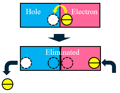
When voltage is applied to the p-n junction so that p becomes plus, the holes and the electrons can be moved toward the interface.
When holes and electrons meet at the interface (junction), the electrons jump into holes and both are eliminated. After those electrons are eliminated, more electrons flow into the n-layer, and electrons flow out from the p-layer, creating new holes. This is repeated, enabling the current to continue to flow.
When voltage is applied in the reverse direction of the p-n junction
-
-
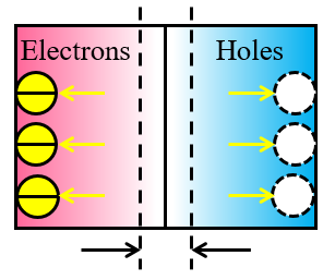
- Here is the region that does not have any holes and electrons…called the depletion layer
-
Voltage is applied to the p-n junction so that n becomes plus.
Since the holes and electrons move away from one another, they do not meet at the interface and the current cannot flow. A region forms close to the interface, called the depletion layer, which does not have any holes and electrons, and this produces voltage-withstanding.
As a result, we know that there is rectification behavior in the p-n junction.

