- TOP
- Lineup
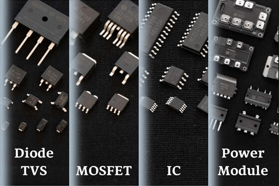
- Semiconductor
- Technical Support
- Technical Data
- Application Note
- MS1003SH / MS1004SH
MS1003SH / MS1004SH
Application Note
Overview/Features
We have developed the MS1003SH and MS1004SH to meet the growing demand for power conservation.
These ICs incorporate a super-standby mode to optimize power efficiency under micro loads.
The MS1003SH and MS1004SH consume less power in standby mode than conventional ICs.
The ICs incorporate various functions to make it more user-friendly and to make it easier to design a power supply with fewer external components.

1. Quasi-resonant design for high efficiency and low noise.
2. Four-step soft-start function.
3. Onboard startup circuit requires no startup resistor, dramatically reducing losses in the startup circuit.
4. The automatic bottom-skip function controls increases in oscillation frequency and improves efficiency under light loads.
5. Auto-burst mode improves efficiency under light loads with no additional components.
6. Super-standby mode improves efficiency under micro loads.
7. Soft drive circuit reduces noise.
8. Thermal shutdown, overvoltage protection, and overload protection (Timer latch)
9. Primary current limit circuit incorporates an input voltage dependence correction circuit to reduce the number of components required.
10. Bias assist function for startup circuit.
11. Vcc-GND short circuit protection function.
12. SOP8/7J package employed for compact dimensions.
Application Note Contents
1. Overview
1.1 Introduction
1.2 Characteristics
1.3 Applications
1.4 Appearance and dimensions
1.5 Basic circuit configuration
2. Block diagram
2.1 Block diagram
2.2 Pin names
3. Circuit operation
3.1 Startup
3.1.1 Startup circuit
3.1.2 Soft-Start (SS)
3.1.3 Bias assist
3.2 Oscillation
3.2.1 On-trigger circuit
3.2.2 Quasi-resonance
3.2.3 Soft drive
3.2.4 Bottom-skip operation
3.2.5 Output voltage control
3.3 Burst operation mode
3.3.1 Auto-burst mode (Auto-atandby mode)
3.3.2 Super-standby mode (SP Standby mode)
3.4 Protection functions
3.4.1 Vcc overvoltage protection latch (OVP)
3.4.2 Overcurrent protection (OCP)
3.4.3 Overload protection (Timer latch circuit)
3.4.4 VCC-GND short circuit protection
3.4.5 Leading edge blank (LEB)
3.4.6 On-trigger malfunction prevention circuit
3.4.7 Thermal shutdown circuit (TSD)
4. Pin functions
4.1 Z/C pin
4.2 F/B pin
4.3 GND pin
4.4 OCL pin
4.5 VG pin
4.6 Vcc pin
4.8 Vin pin
5. Design procedure
5.1 Design flow chart
5.2 Example of main transformer design conditions
5.3 Formulas for main transformer design
5.4 Checking the operating points
5.4.1 Variables in formulas
5.4.2 Bottom-skip start power
5.4.3 Bottom-skip end power
5.4.4 Auto-burst start/end power
5.4.5 Drooping- point power
5.5 Pin design
5.5.1 Z/C pin (Pin 1)
5.5.2 F/B pin (Pin 2)
5.5.3 OCL pin (Pin 4)
5.5.4 VG pin (Pin 5)
5.5.5 Vcc pin (Pin 6)
5.5.6 Setting resonating capacitor
6. Example circuit diagram
6.1 Circuit diagram
6.2 Calculations for example circuit design
Example Circuits

| Terms and Conditions for Licensing of Application Note |
|
Upon downloading Application Note, you will be considered as having given your consent to the content of this Agreement. |
|