- TOP
- Lineup
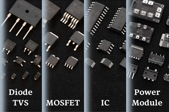
- Semiconductor
- Learn about product features
- Ideal diode ICs
Ideal diode ICs
▼MF2003SV V-DiodeTM
Pch_MOSFET with built-in reverse current protection function
Achieves low dissipation and downsizing
▼MF2007SW
An Nch_MOSFET gate driver IC
with built-in reverse current protection function

Pch_MOSFET with built-in reverse current protection function
Achieves low dissipation and downsizing
MF2003SV V-DiodeTM

■Achieves low dissipation and downsizing compared to conventional diodes (SBD).
■Equipped with active clamp function
■Compact package
■Based on AEC-Q100
■Equipped with active clamp function
■Compact package
■Based on AEC-Q100
Heat generation/Dissipation reduction
Reduction of heat generation and dissipation.
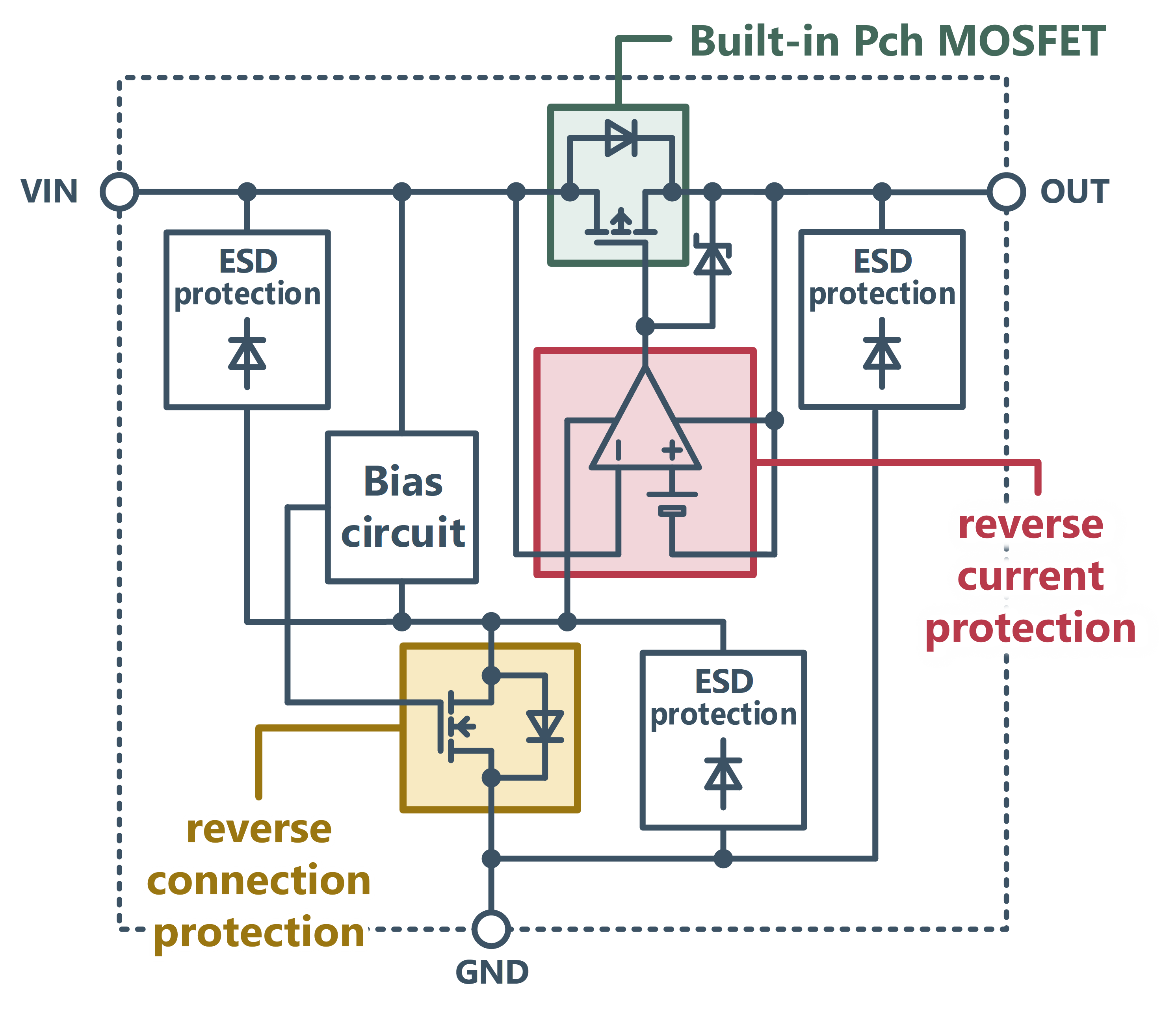
Built-in MOSFET Ron≒57mΩ
Equipped with active clamp function
Equipped with function which clamps at approximately ∆VDS≈40V to prevent breakdown of the built-in Pch MOSFET.
Compact package
Utilizes a WSON8-4040 (4.0mm x 4.0mm) leadless package with wettable flank terminals.
Block Diagram
Product Specifications
| MF2003SV | |
|---|---|
| Package | WSON8-4040 |
| Operating voltage | 2.5 to 40V |
| Average current | 5A |
| Quiescent current | ≦3μA |
| Built-in Pch MOSFET Ron | 53mΩ(Typ.) |
| Reverse connection protection | Built-in |
| Reverse current protection | Built-in (25mV offset comparator) |
| IFSM | 70A |
| Toff | 500ns(Typ.) |
An Nch_MOSFET gate driver IC
with built-in reverse current protection function
MF2007SW

■Heat generation/Dissipation reduction
■Selectable reverse current protection function
■Wide input voltage range
■Selectable reverse current protection function
■Wide input voltage range
Heat generation/dissipation reduction
Aims to reduce heat generation and dissipation compared to SBD by utilizing MOSFET.
Heat generation and dissipation are dependent upon externally connected Nch_MOSFET.
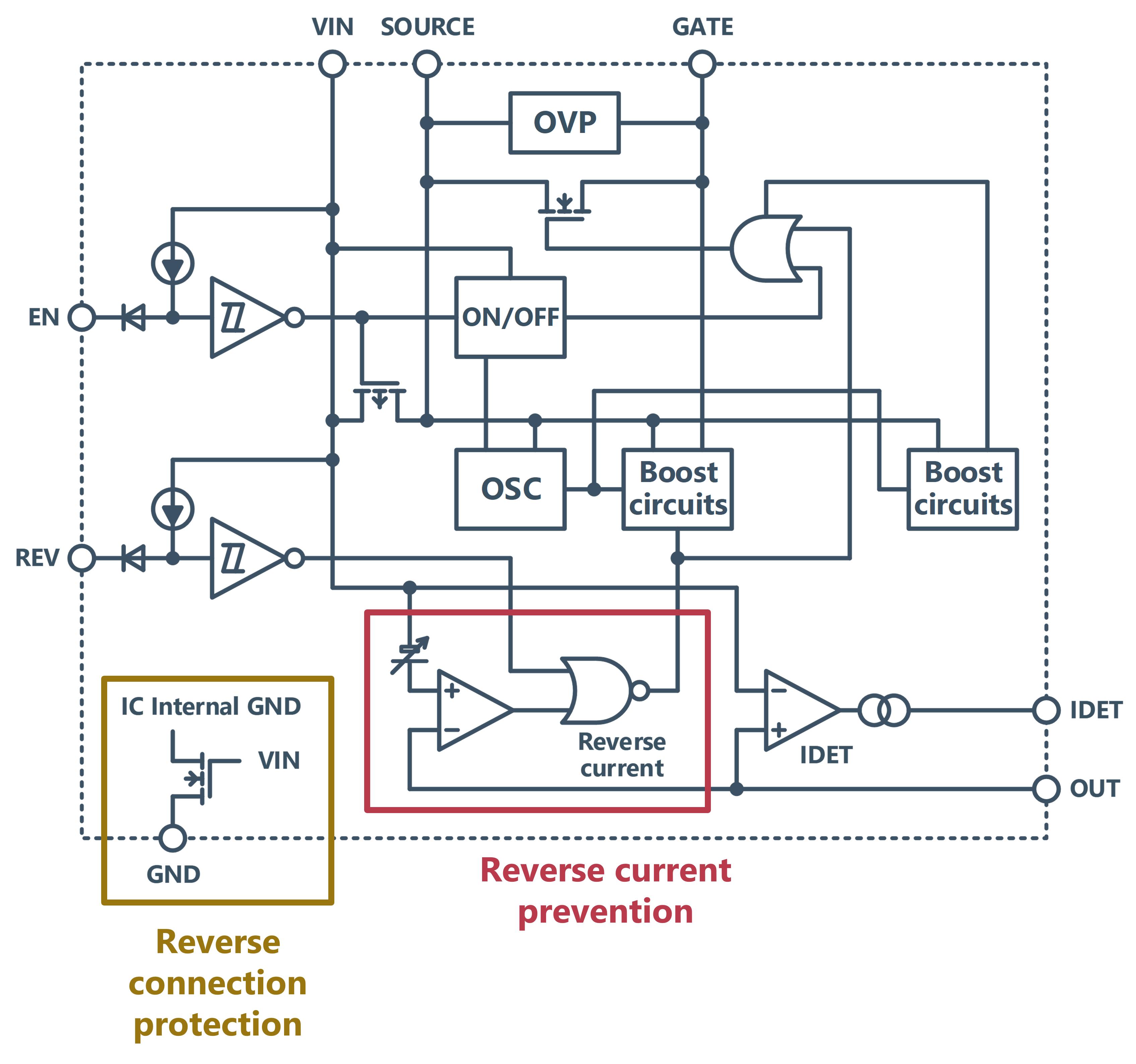
Wide input voltage range
Compatible with a wide range of input voltages from 4.5 to 65V, which allows for use in a wide range of devices.
Selectable reverse current protection function
The reverse current protection function can be switched ON and OFF via the REV terminal Hi/Lo status.
No function : Bidirectional conduction is possible.
Block Diagram
Product Specifications
| MF2007SW | |
|---|---|
| Package | TSSOP10 |
| Operating voltage | 4.5 to 65V |
| Standby current | ≦5μA (external signal) |
| Booster circuits output current | 75μA(Typ.) |
| Boost voltage | 12.5V(Typ.) |
| Reverse current_OFF time | 200ns/0.7A(Typ.) |
| EN_OFF time | 50ns/0.12A(Typ.) |
| When the power supply is connected in reverse | Current reduction, External gate discharge |
| Charge pump | Built-in capacitor |