- TOP
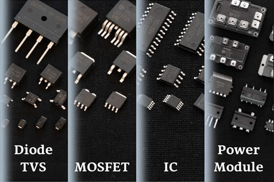
- Lineup
- Semiconductor
- Learn about product features
- Low withstand voltage MOSFETs
Low withstand voltage MOSFETs
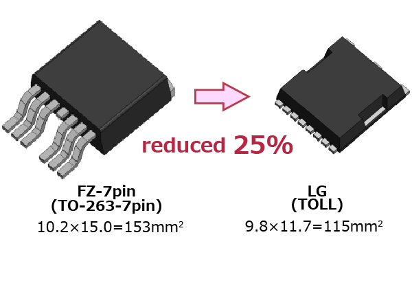
▼LG(TOLL)package
Medium withstand voltage of 100V to 200V newly deployed in a compact, thin package!
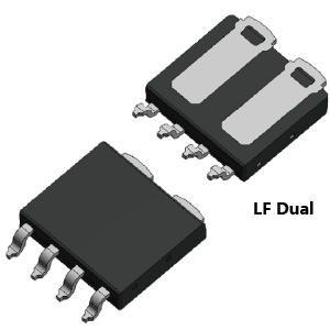
▼Dual MOSFET
Two low dissipation power MOSFET elements in 1 package,
Contributes to circuit downsizing and weight reduction
▼EETMOS 5 series
This series greatly improves upon the trench gate structure to achieve low Qg and low noise
▼EETMOS 3/4 series
Cu clip structure achieves low Ron and large current
40V to 120V low withstand voltage MOSFETs
▼EETMOS 3 series
Optimized trench gate structure and trench layout,
23% Ron・A reduction

Medium withstand voltage of 100V to 200V
newly deployed in a compact, thin package!
LG(TOLL)package
[ under development ]

■Contributing to device downsizing and increased efficiency through low Ron
■Mounting area reduced by approximately 25% compared to D2PAK(TO-263)
■Tch=175°C Expansion of automotive application/reduced size and slim package
JEDEC PKG Code MO-299B
■250A ultra high current devices
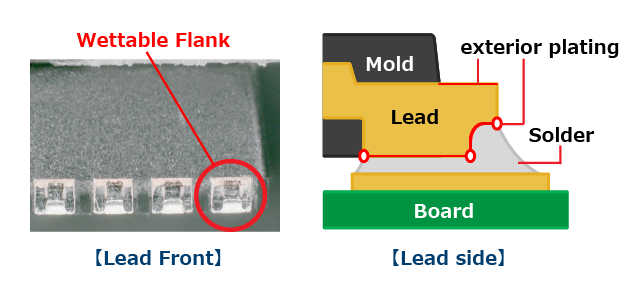
■Use of a wettable flank structure makes compatibility with automatic appearance inspections after mounting possible
■Products can also be developed with Kelvin source terminals to reduce switching loss
■Mounting area reduced by approximately 25% compared to D2PAK(TO-263)
■Tch=175°C Expansion of automotive application/reduced size and slim package
JEDEC PKG Code MO-299B
■250A ultra high current devices
■Use of a wettable flank structure makes compatibility with automatic appearance inspections after mounting possible
■Products can also be developed with Kelvin source terminals to reduce switching loss
Contributes to device downsizing
Mounting area reduced by approximately 10% compared to conventional conventional package(D2PAK(TO-263)).These features can contribute to equipment downsizing.
Compatible with automatic appearance inspections
Products can also be developed with Kelvin source terminals to reduce switching loss.
Product Specifications
| Part Name | VDS min. [V] | ID max. [A] | VTH typ. [A] | Ron [mΩ]※1 | Ciss(typ.)※2[pF] | Coss(typ.)※2[pF] | Crss(typ.)※2[pF] | Status | |
|---|---|---|---|---|---|---|---|---|---|
| typ. | max. | ||||||||
| P280LG4GNK | 40 | 280 | 3.0 | 0.44 | 0.55 | 23500 | 4800 | 750 | Planning |
| P280LG6GNK | 60 | 280 | 3.0 | 0.61 | 0.77 | 14630 | 6074 | 277 | Planning |
| P232LG10GNK | 100 | 232 | 3.0 | 1.29 | 1.62 | 9325 | 4170 | 128 | RS |
| P166LG15GNK | 150 | 166 | 3.0 | 3.56 | 4.45 | TBD | TBD | TBD | Planning |
| P120LG20GNK | 200 | 120 | 3.0 | 7.8 | 9.8 | 5822 | 447 | 27 | RS |
※1 VGS=10V
※2 VDS=25V
※2 VDS=25V
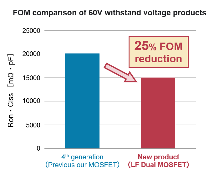
Two low dissipation power MOSFET elements in 1 package,
Contributes to circuit downsizing and weight reduction
Dual MOSFET
[ under development ]
■40V to 100V low withstand voltage Dual MOSFETs
■Two low dissipation power MOSFET elements in 1 package
■Equipped with new structure MOSFET achieves even greater characteristic improvements over Shindengen conventional products
■ 5×6 mm size package(Can replace SOP8 and HSON types)
■Achieves low Ron and downsizing
■Alleviates substrate stress
■Improves solder wettability and provides high reliability
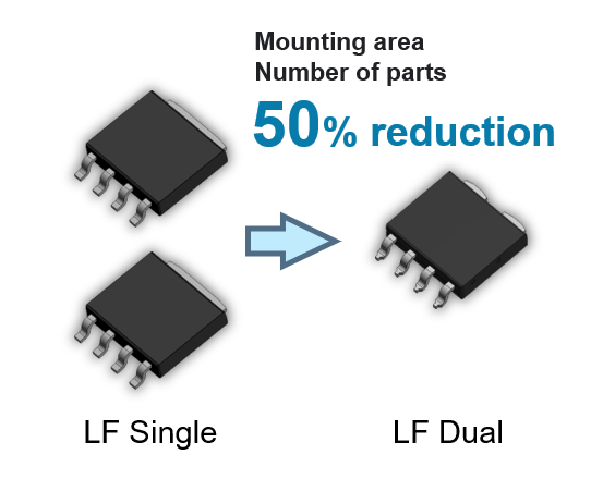
This contributes to circuit downsizing and weight reduction
Allows for a reduction in mounting area and number of components compared to use of two 1 element devices.
This contributes to circuit downsizing and weight reduction.
This contributes to a reduction in switching loss
Reduction of capacity from Shindengen conventional products reduces FOM (Ron×Ciss) by 25%.This allowed for even greater characteristics improvement over Shindengen conventional products.
Achieves downsizing and reduced Ron
Achieves downsizing and reduced Ron through a substantial shift to low resistance and improved heat dissipation.
Realizes high reliability mounting
Alleviates substrate stress while the wettable flank structure improves wettability visibility to provide higher reliability.
Product Specifications
| Part Name | VDS min. [V] | ID max. [A] | VTH typ. [A] | Ron [mΩ]※1 | Series | |
|---|---|---|---|---|---|---|
| typ. | max. | |||||
| P20LF4QTKD | 40 | 20 | 2.0 | 12.3 | 15.3 | EETMOS®4 |
| P41LF4QTKD | 40 | 41 | 2.0 | 5.3 | 6.7 | EETMOS®4 |
| P50LF4QTKD | 40 | 50 | 2.0 | 4.4 | 5.5 | EETMOS®4 |
| P15LF6QTKD | 60 | 15 | 2.0 | 24.0 | 30.0 | EETMOS®4 |
| P33LF6QTKD | 60 | 33 | 2.0 | 10.0 | 12.5 | EETMOS®4 |
| P33LF6QLKD | 60 | 33 | 2.0 | 10.5 | 13.1 | EETMOS®4 |
| P39LF6QTKD | 60 | 39 | 2.0 | 8.3 | 10.4 | EETMOS®4 |
| P12LF10SLKD | 100 | 12 | 2.0 | 34.0 | 42.0 | EETMOS®3 |
| P17LF10SLKD | 100 | 17 | 2.0 | 29.0 | 36.0 | EETMOS®3 |
※1:VGS=10V
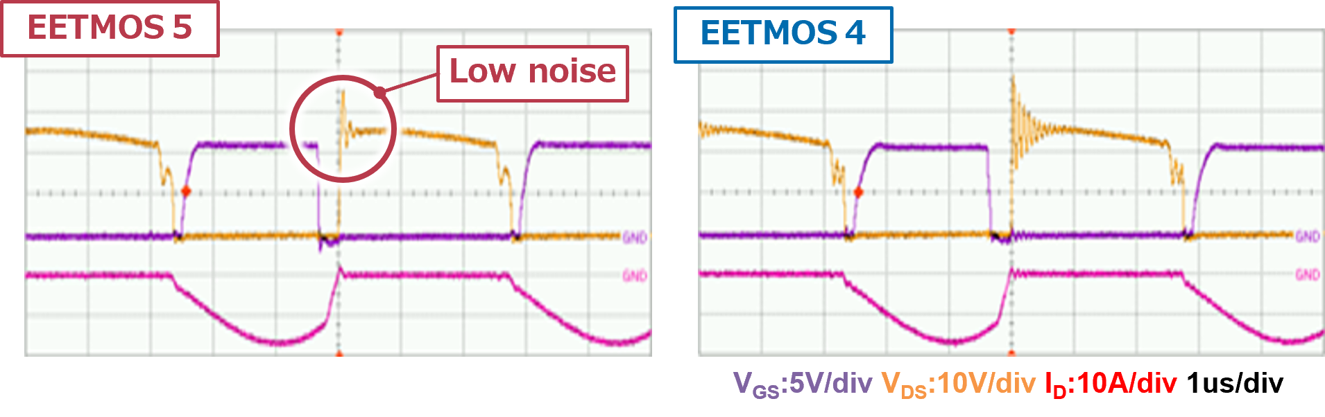
This series greatly improves upon the trench gate structure to
achieve low Qg and low noise.
EETMOS 5 series
[ under development ]

■40V to 200V low withstand voltage MOSFETs
■This series greatly improves upon the trench gate structure of the conventional EETMOS 4 series to achieve low Qg and low noise
■Cu clip structure achieves low Ron and downsizing
■This series greatly improves upon the trench gate structure of the conventional EETMOS 4 series to achieve low Qg and low noise
■Cu clip structure achieves low Ron and downsizing
Achieves low Qg and low noise
This series greatly improves upon the trench gate structure of the conventional EETMOS 4 series to achieve low Qg and low noise.Comparison of power supply synchronous rectified waves.
Low Ron and low Qg effects achieve low dissipation and high efficiency
Comparison carried out with conventional processes as 1. Reduced power consumption by 37% in the VDS=40V class and by 46% in the VDS=200V class.
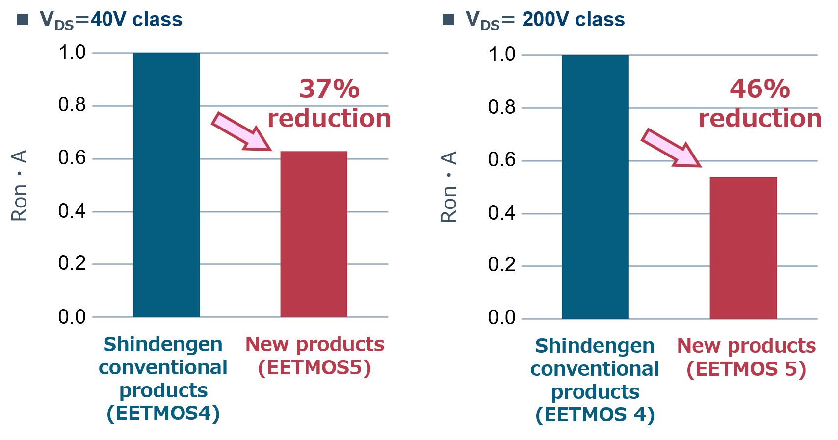
Achieves low Ron and low Qg
Low Ron and low Qg effects achieve low dissipation and high efficiency.
(Compared to conventional EETMOS 4 under same chip conditions)
Product Specifications
LF package (5×6mm)
| Part Name | VDS min. [V] | ID max. [A] | VTH typ. [A] | Ron [mΩ]※1 | Series | |
|---|---|---|---|---|---|---|
| typ. | max. | |||||
| P180LF4GNK | 40 | 180 | 3.0 | 1.01 | 1.23 | Planning |
| P120LF6GNK | 60 | 120 | 3.0 | 1.60 | 2.00 | RS |
| P74LF10GNK | 100 | 74 | 3.0 | 4.90 | 6.20 | Planning |
| P36LF20GNK | 200 | 36 | 3.0 | 20.70 | 25.90 | Planning |
FZ-7p package (TO-263SC)
| Part Name | VDS min. [V] | ID max. [A] | VTH typ. [A] | Ron [mΩ]※1 | Series | |
|---|---|---|---|---|---|---|
| typ. | max. | |||||
| P240FZ4GNKA | 40 | 240 | 3.0 | 0.85 | 1.07 | Planning |
| P240FZ6GNKA | 60 | 240 | 3.0 | 0.91 | 1.20 | Planning |
| P130FZ10GNKA | 100 | 130 | 3.0 | 3.70 | 4.60 | Planning |
| P58FZ20GNKA | 200 | 58 | 3.0 | 14.30 | 17.90 | Planning |
LG package (TOLL)
| Part Name | VDS min. [V] | ID max. [A] | VTH typ. [A] | Ron [mΩ]※1 | Series | |
|---|---|---|---|---|---|---|
| typ. | max. | |||||
| P280LG4GNK | 40 | 280 | 3.0 | 0.50 | 0.63 | Planning |
| P280LG6GNK | 60 | 280 | 3.0 | 0.77 | 0.96 | Planning |
| P232LG10GNK | 100 | 232 | 3.0 | 1.83 | 2.20 | RS |
| P85LG20GNK | 200 | 85 | 3.0 | 8.70 | 10.90 | RS |
※1:VGS=10V
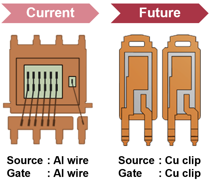
Cu clip structure achieves low Ron and large current
40V to 120V low withstand voltage MOSFETs
EETMOS 3/4 series

■40V to 120V low withstand voltage MOSFETs
■5×6mm exterior (can replace SOP8 and HSON types)
■Cu clip structure achieves low Ron and large current(up to 140A)
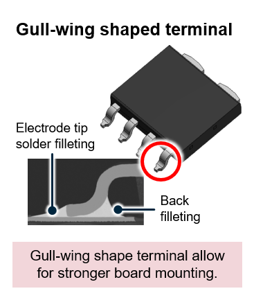
■Use of gull-wing shape for one side of lead alleviates substrate stress
■Plating of the lead tip improves solder wettability and provides high reliability
■5×6mm exterior (can replace SOP8 and HSON types)
■Cu clip structure achieves low Ron and large current(up to 140A)
■Use of gull-wing shape for one side of lead alleviates substrate stress
■Plating of the lead tip improves solder wettability and provides high reliability
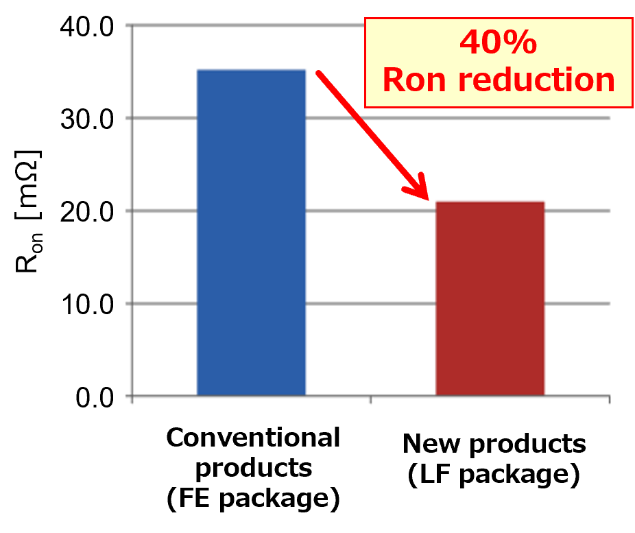
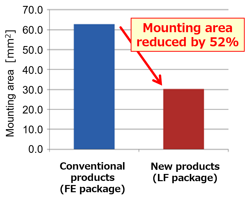
Achieves downsizing and reduced Ron resistance
Uses a Cu clip structure which significantly reduces low resistance and improves heat dissipation, reduces Ron by 40% compared to Shindengen conventional products, and also reduces mounting area by 52%.
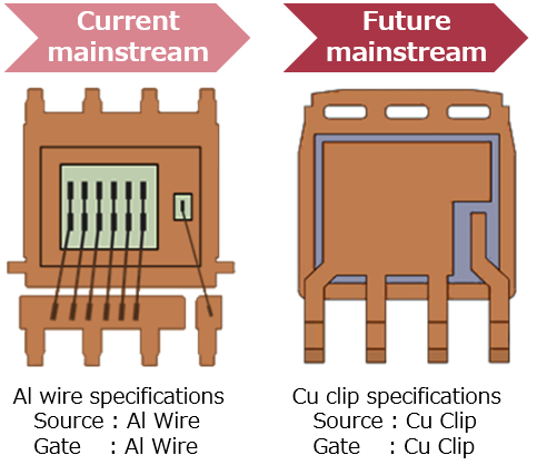
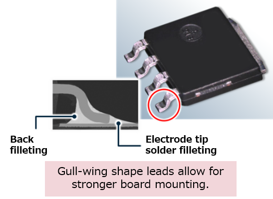
Strong board mounting
Gull-wing shaped leads allow for stronger board mounting,
Product Specifications
LF package (5×6mm)
| Part Name | VDS min. [V] | ID max. [A] | VTH typ. [A] | Ron [mΩ]※1 | Series | |
|---|---|---|---|---|---|---|
| typ. | max. | |||||
| P24LF4QLK | 40 | 24 | 2.0 | 9.60 | 12.0 | MP |
| P70LF4QLK | 40 | 70 | 2.0 | 3.60 | 4.50 | MP |
| P105LF4QLK | 40 | 105 | 2.0 | 2.10 | 2.70 | MP |
| P140LF4QLK | 40 | 140 | 2.0 | 1.17 | 1.42 | MP |
| P18LF6QLK | 60 | 18 | 2.0 | 21.0 | 26.0 | MP |
| P38LF6QLK | 60 | 38 | 2.0 | 7.90 | 9.90 | MP |
| P64LF6QLK | 60 | 64 | 2.0 | 4.50 | 5.70 | MP |
| P98LF6QLK | 60 | 98 | 2.0 | 2.50 | 3.20 | MP |
| P46LF7R5SLK | 75 | 46 | 2.0 | 8.20 | 10.30 | MP |
| P72LF7R5SLK | 75 | 72 | 2.0 | 4.60 | 5.80 | MP |
| P32LF10SLK | 100 | 32 | 2.0 | 15.70 | 19.70 | MP |
| P50LF10SLK | 100 | 50 | 2.0 | 9.00 | 11.30 | MP |
| P25LF12SLK | 120 | 25 | 2.0 | 23.00 | 29.00 | MP |
| P40LF12SLK | 120 | 40 | 2.0 | 13.00 | 16.30 | MP |
FZ-7p package (TO-263SC)
| Part Name | VDS min. [V] | ID max. [A] | VTH typ. [A] | Ron [mΩ]※1 | Series | |
|---|---|---|---|---|---|---|
| typ. | max. | |||||
| P240FZ4QNKA | 40 | 240 | 3.0 | 1.01 | 1.27 | MP |
| P170FZ6QNKA | 60 | 170 | 3.0 | 1.94 | 2.50 | MP |
※1:VGS=10V
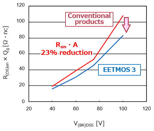
Optimized trench gate structure and trench layout.23% Ron・A reduction
EETMOS 3 series

■40~120V MOSFET
■Optimized trench gate structure and trench layout
■23% Ron・A reduction compared to conventional types
■LA(5×6), FB(TO-252), FP(TO-263Adv.), FTO-220AG
■Optimized trench gate structure and trench layout
■23% Ron・A reduction compared to conventional types
■LA(5×6), FB(TO-252), FP(TO-263Adv.), FTO-220AG
Achieve 23% Ron・A reduction
100V products achieve 23% Ron・A reduction compared to conventional types.
Product Specifications
| Part Name | VDS min. [V] | ID max. [A] | Ron [mΩ]※1 | Series | |
|---|---|---|---|---|---|
| typ. | max. | ||||
| P24B4SB | 40 | 24 | 14.8 | 18.5 | FB |
| P60B4SN | 40 | 60 | 3.2 | 4.0 | FB |
| P16B6SB | 60 | 16 | 29.0 | 37.0 | FB |
| P60B6SN | 60 | 60 | 5.3 | 6.7 | FB |
| P8B10SB | 100 | 8 | 75.0 | 94.0 | FB |
| P40B10SN | 100 | 40 | 13.4 | 16.8 | FB |
| P32B12SN | 120 | 32 | 20.0 | 25.0 | FB |
| P24B15SL | 150 | 24 | 33.0 | 42.0 | FB |
| P86F6SN | 60 | 86 | 2.4 | 3.0 | FTO-220AG |
| P66F7R5SN | 75 | 66 | 4.0 | 5.0 | FTO-220AG |
| P82F7R5SN | 75 | 82 | 3.0 | 3.8 | FTO-220AG |
| P22F10SN | 100 | 22 | 22.0 | 28.0 | FTO-220AG |
| P40F10SN | 100 | 40 | 8.5 | 10.7 | FTO-220AG |
| P50F10SN | 100 | 50 | 6.9 | 8.7 | FTO-220AG |
| P32F12SN | 120 | 32 | 12.4 | 15.5 | FTO-220AG |
| P40F12SN | 120 | 40 | 9.5 | 11.9 | FTO-220AG |
※1:VGS=10V