- TOP
- Lineup
- New Product
- Notice of commencement of shipping for samples of the MF2001SF industry minimum low input voltage driven IC
New Product
Notice of commencement of shipping for samples of the MF2001SF industry minimum low input voltage driven IC
Apr. 7, 2017
1. Overview
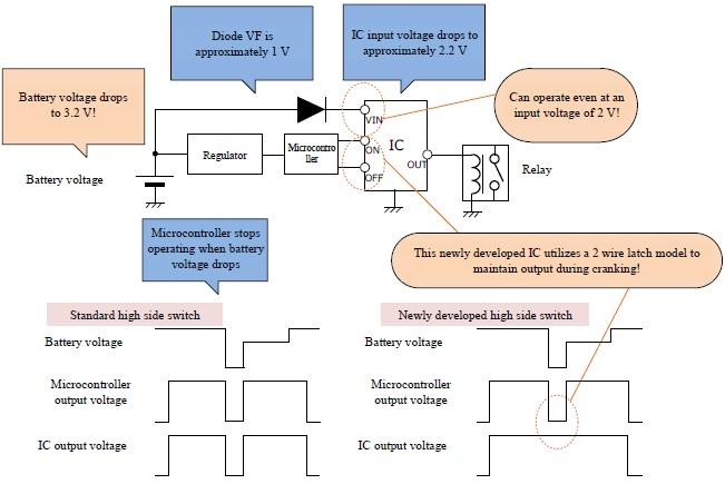
There has been a recent focus on measures for operation at low input voltages in order to avoid devices being unable to function correctly as a result of drops in battery voltage which occur when an automobile restarts from a cold cranking or idling stop.
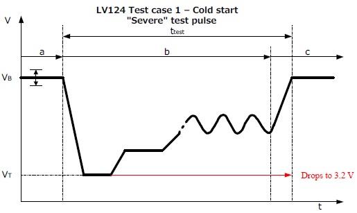
The newly developed MF2001SF achieves an industry best low input voltage of 2 V and is compatible with the LV124 cold cranking conditions (battery voltage drop to 3.2 V) established by German automobile manufacturers, allowing devices to operate correctly even when battery voltage drops.
The device is also a high side drive control IPD with built-in Pch high withstand voltage power MOSFET that is also compatible with wide input voltage range of 2 V to 42 V developed using Shindengen's proprietary technologies.
2. Features
- Achieves the industry's best low voltage input of 2 V
- Compliant with LV124 cold cranking conditions (drop in battery voltage to 3.2 V)
- Utilizes a 2 wire latch model which makes it possible to maintain output during cranking
- Wide input voltage range: DC 2 V to 42 V
- Safety design: Will not be damaged by adjacent pin shorts, etc.
3. Specifications
| Input voltage drive | Can operate from 2 V |
|---|---|
| Wide input voltage range | DC 2 V to 42 V |
| Standby current (dark current) | 20 μA typ. |
| Operation mode | Drive signal 2 wire (Latch model: Enables maintenance of output even when output from the microcontroller etc. stops) |
| Output Pch MOSFET current | 1 A max |
| Output Pch MOSFET ON resistance | 330 mΩ typ. |
| Built-in protection functions | Overcurrent protection, overheat protection |
| Junction temperature | Tj max = 150°C |
| Recovery after short detection | Automatic recovery |
4. Typical Applications
Battery direct linked high side switches (for relay drive)
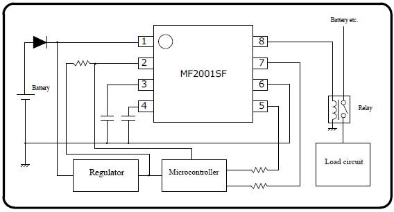
5. Basic Circuit Configuration
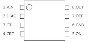
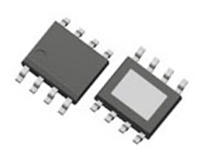
6. Pin Arrangement / Exterior Diagram (HSOP-8N Package)
| Pin No. | Symbol | Function |
|---|---|---|
| 1 | VIN | Power supply pin |
| 2 | DIAG | Output status notification pin |
| 3 | CT | Short output monitoring timer |
| 4 | CRT | Automatic recovery timer |
| 5 | ON | High side ON pin |
| 6 | GND | Ground pin |
| 7 | OFF | High side OFF pin |
| 8 | OUT | Output pin |
7. Inquiries
Shindengen Electric Manufacturing Co., Ltd.
Marketing & Sales Dept. Sales Div. Group
e-mail: dendeba@shindengen.co.jp
* Content accurate as of April, 2017.
8. Notes
- The content of these materials may be changed at any time without prior notice for product improvements or other reasons.
- Our company shall not be held responsible or liable for any damages, or infringement of patents or other rights which occur as a result of the use of these materials.
- Reproduction of any portion of these materials without prior written authorization is strictly prohibited.
Please note that the information contained in releases is current as of the date of press announcement, but may be subject to change without prior notice.
Relation Contents
-

Application
Introductions to fields in which Shindengen products are used.
-
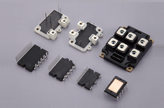
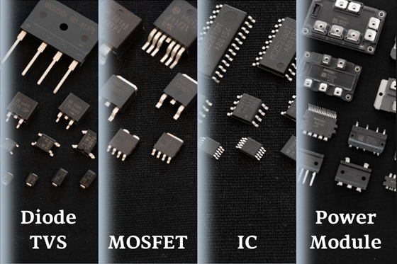
Semiconductor
Introductions to Shindengen semiconductor products information.
-
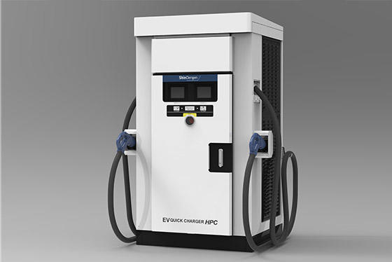
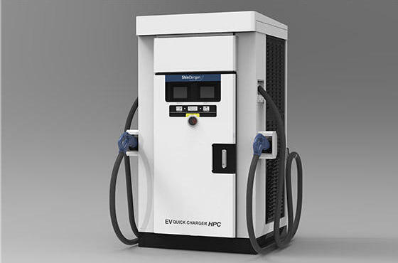
Environment and Energy Products
Introductions to Shindengen environment and energy products.
-
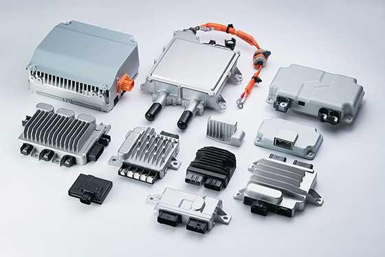
Power Management Electronics
Introductions to Shindengen Power Management Electronics Products information.