
Value Creation
Technology and Development Center
Overview of the Technology and Development Center
The Technology and Development Center handles the basic research and applied research development stages that come before product commercialization. Technological challenges we are working on include developing elemental and module mounting technologies that are indispensable for low-loss devices as well as IC product process technologies and high-efficiency, low-noise power supply circuits. Using simulations, we determine the properties and key points of technologies in development, accumulating knowledge in order to efficiently pass on the results of our work to the business divisions, shifting from forward-looking elemental technology development to practical mass production design. The product development departments in each segment then coordinate with sales and marketing departments to use these technologies to develop new products optimized for the needs of their markets and customers.
■Progress under the Medium Term Business Plan
Focusing on the 15th Medium Term Business Plan’s strategy of “Create next-generation products that are a decade ahead,” we are developing technologies that are needed by our operating departments or across departments.
In semiconductor devices, we are focusing primarily on the development of low loss technologies, high-speed and high-temperature operation, and mounting technologies for components that integrate multiple chips and elements. In power electronics, we are advancing development mainly in the areas of high-efficiency technologies, high-density mounting technologies and lowering noise. Furthermore, in order to expand into new business areas, we are advancing development with external research institutions. By solving these research challenges and realizing synergies leveraging our core technologies, we are working to improve product competitiveness and rapidly develop new products suited to market needs and applications.
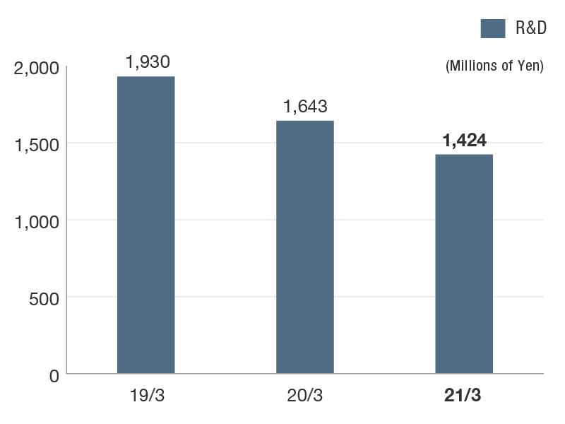
R&D
R&D expenses under the medium-term plan were as follows.
R&D and Capital Investment
Highlights
Initiatives in Next-Generation Devices
One of our initiatives in next-generation devices is R&D using not only silicon carbide (SiC) and gallium nitride (GaN), but beta-gallium oxide. Compared with SiC or GaN, devices using beta-gallium oxide can more easily handle high voltage and high current and offer advantages in terms of eco-friendliness. They are also expected to offer an advantage over other silicon alternatives in terms of the cost of semiconductor fabrication processes.
In addition to existing silicon power devices, Shindengen is committed to proactively developing next-generation low-loss power semiconductors using new materials, namely SiC, GaN and now beta-gallium oxide. By maximizing energy conversion efficiency, we will contribute to the realization of a low-carbon society.
Launch of the FPD Department
One of the strategies of the Medium Term Business Plan is to “Create next-generation products that are a decade ahead.” In pursuit of this strategy and to further reinforce the activities of the Future Strategy Committee established two years ago, we have now established the Future Products Development (FPD) Department. Focused on R&D outside the bounds of existing businesses, the department is working to generate innovation over the medium to long term and accelerating initiatives that will lead to future product commercialization.